Precision positioning for electronics
Challenge
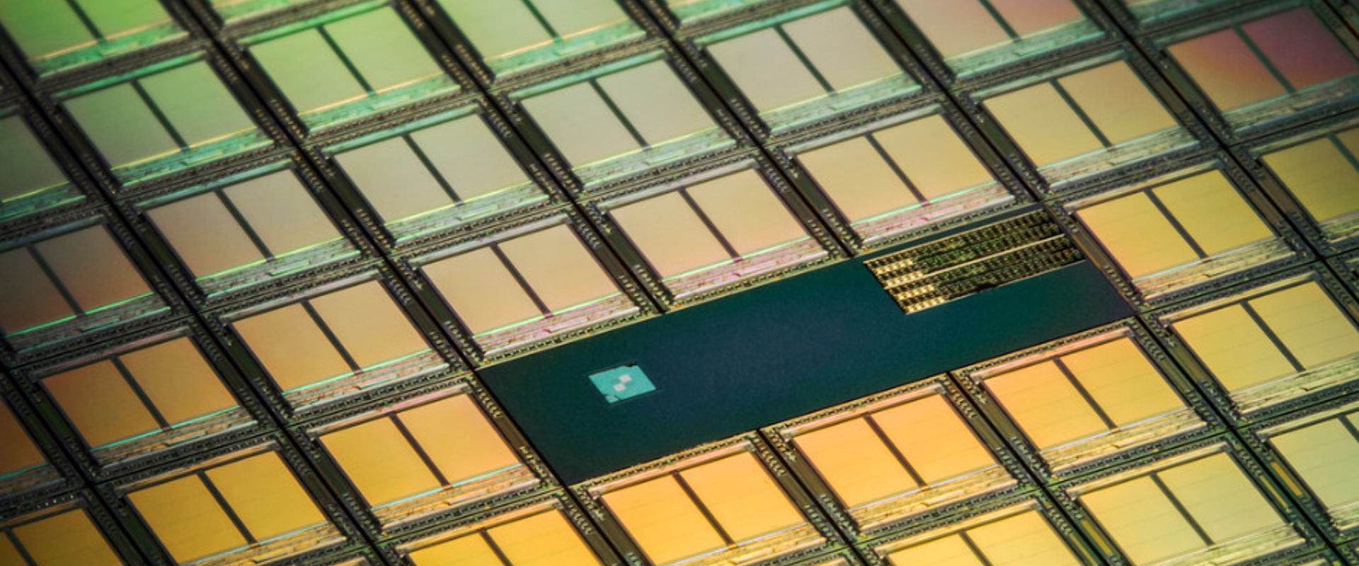
Producing circuits on silicon wafers relies on high-precision manufacturing processes that assemble electronic components to form multiple complete circuits on a single wafer. These are later separated into individual units for device assembly. To improve productivity and efficiency, wafer manufacturers are investigating methods to increase circuit production by fabricating more circuits on larger wafers.
During manufacture, positioning stages move wafers in 3D inside a vacuum chamber, as tiny details are etched or deposited onto them, to build-up electronic circuits. Achieving the high levels of position control required relies on accurate movement sensing techniques able to operate in challenging industrial environments. As more features are added to wafers, the distance between individual components shrinks and ever greater control over the stage’s nanometre movement are essential.
Interferometry is a laser-based technique for precisely determining distances in a single direction. It is based on splitting a laser beam into two, one beam travels to and is reflected back from a target on the item that moves, while the other acts as a reference. Recombining the two creates an interference pattern that can be used to accurately determine position changes. Currently multiple lasers are needed to generate information for movements in 3D, adding complexity and introducing significant measurement errors. To overcome these problems more powerful lasers able to generate multiple intense beams for 3D measurements, coupled with system simplification, are needed to enable industrial users to benefit from highly accurate interferometry measurements.
Solution
The EMRP Project, Metrology for movement and positioning in six degrees of freedom, developed a powerful infrared laser, suitable for making 3D interferometry measurements.
The new laser, which was characterised in the project, is 10 times more powerful than lasers currently used in measurement applications. This increased power allows a single laser light source to be split into multiple beams of sufficient intensity for use in simultaneously determining movements in 3D.
Impact
TESCAN, a Czech company manufacturing scanning electron microscopes and advanced analysis instrumentation, is upgrading the laser technology demonstrated in the project, for incorporation into a new wafer manufacturing system they are developing for electronic circuit production. Tescan’s system will incorporate a positioning stage, based on their existing technology, to provide the highly controlled nanoscale movements for silicon wafer production. Determining the precise position of the stage will be achieved using the project evaluated high powered laser and an interferometry system capable of operation in 3D.
New innovations in positioning technology, such as the extension of interferometry for use in 3D, are vital for improving production speed and efficiency in many industries. Increasing the precision of nano-positioning is supporting the development of a new European silicon wafer production capability and has the potential to reduce European industrial reliance on external suppliers as the demand for more sophisticated electronics grows.
- Category
- EMRP,
- Industry,
