Please type a search term (at least two characters)
News
EURAMET consults stakeholders from the semiconductor sector

The Metrology Network for Advanced Manufacturing takes a leap forward in preparation for the European Chips Act
With the European Chips Act, the EU considers semiconductor shortages and aims to strengthen Europe’s technological leadership by creating a state-of-the-art chip ecosystem that covers the whole value chain. In that prospect, outstanding metrological solutions need be developed to address the emergent technological innovations relying on measurement science in areas ranging from research & design to industrial testing & production.
EURAMET- the European Association of National Metrology Institutes - is the primary voice promoting measurement science and its application in Europe. Alongside the other pillars of the international quality infrastructure fostering sustainable economic development, EURAMET aims at raising awareness and promoting strategic cooperation with actors from key societal and industrial sectors. In order to engage with its various groups of stakeholders and further respond to their particular necessities, EURAMET founded the European Metrology Networks (EMNs) encompassing fields such quantum technologies, environmental monitoring and energy transition. Amongst them, the EMN for Advanced Manufacturing provides the high-level coordination of initiatives and activities within the metrology community, all the while nurturing the impact of specific developments for the areas of advanced materials, smart manufacturing systems and manufactured components & products.
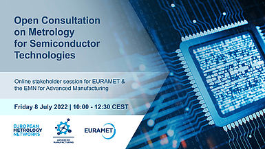
EURAMET and the Advanced Manufacturing network organised an Open Consultation on Metrology for Semiconductor Technologies aimed at gathering metrological needs and challenges identified by major players in the chip ecosystem. The event, held online on 8 July 2022, was attended by over a hundred participants from the semiconductor industry, universities, research centres, the political sphere and calibration laboratories together with numerous EURAMET members and associates. The guest speakers represented R&D institutes and manufacturing companies - ASML, IMEC, ZEISS, STMicroelectronics - alongside the Key Digital Technologies Joint Undertaking, a Public-Private European Partnership for research, development & innovation which funds projects to foster world-class expertise in key enabling technologies that are essential for Europe's competitive leadership.
The speakers are involved in projects addressing a broad spectrum of sectors, from advanced 2D materials for enhanced device performance, future CMOS and ‘More-than-Moore’ technologies which go beyond device scaling concepts, to integrated high volume manufacturing systems in semiconductor fabs worldwide. They listed multiple examples of where state-of-the-art metrology must be developed and integrated into the production chain, both at the research and development laboratories and within the manufacturing stream:
- optical and e-beam patterning, characterisation and control of lithographic scanner to enable optimal system settings and patterning performance, feature placement metrology, after-etch profilometry
- 3D extension of the integrated circuit technology via wafer-to-wafer and chip-to-chip bonding
- accurate solutions for reflectivity metrology of high NA EUV mirrors coated with multilayers as well as micro-interferometry for roughness characterisation of mirrors over larger surfaces
- future CMOS and beyond CMOS: faster time to data on more complex structures, development of correlative approaches, integration of 2D materials into the process flow
- characterisation of advanced materials & system architectures: optical material parameters, mechanical and thermal properties of components; stress, adhesion and piezoelectrical behaviour
- mathematical tools and concepts that complement the more traditional metrological approaches: smart sampling methods, statistical algorithms and artificial intelligence
One of the predominant conclusions of the event was that metrological services must progress, for example through transdisciplinary research and improved infrastructure, to keep up with the fast-evolving pace of the semiconductor industry. Messages conveyed by the speakers coalesced around the need for more precise measuring instrumentation, faster test methods and analysis techniques that support the learning cycle, optimisation and on-the-spot quality control that further enables quick and reliable decision making.
Dr. Harald Bosse (PTB, Germany), Chair of the EMN for Advanced Manufacturing, further explained about this event:
“The outcomes of the consultation around future breakthroughs in metrology for the semiconductor technologies will be fed into the EMN Advanced Manufacturing Strategic Research Agenda, complementing the fruits of other approaches to identify existing and upcoming trends in metrology to support European advanced manufacturing. For example, the perspectives illustrated through the in-depth overview published in Measurement Science and Technology coupled with the insights from the 2021 stakeholder plenary meeting are incorporated into this road-mapping process”.
These efforts will lay the foundation for upcoming collaboration initiatives and also guide the development of future calls for joint research projects within the European Partnership on Metrology and beyond.
Want to hear more about EURAMET?
Carbon dioxide, released from man-made activities, is lowering the pH of the Earth’s oceans, and impacting the health of marine organisms worldwide more
Supporting automated and reconfigurable manufacturing systems more
Working with external project Cool White to test and suggest improvements on the locally available white paints more
The project FutureEnergy has provided new calibration services for ultra-high voltages and a good practice guide on Lightning Impulse dividers more
For many of the 5000 photonics companies in Europe a precise knowledge of a material’s optical properties is vital for industrial competitiveness more


