- About EURAMET
- Research & Innovation
- Metrology for Society's Challenges
- World Metrology Day 2023
- Case Studies
- EURAMET's contribution to the COVID-19 response
- SI redefinition
- World Metrology Day 2021
- Metrology for Energy
- Metrology for Health
- Metrology for Environment
- Metrology for Industry
- Measurements for New Technologies
- Future measurement standards
- Metrology and Standardisation
- EMRP Achievements
- Impact
- Technical Committees
- European Metrology Networks
- Knowledge Transfer
- Publications & Media Centre
- Search Contacts
- Publications Repository Link
Please type a search term (at least two characters)
News
EMPIR project develops new silicon device and measurement guidelines
Company licences two patent applications; best practice guide available
Recently completed EMPIR project <link research-innovation search-research-projects details>‘Metrology for the photonics industry – optical fibres, waveguides and applications’ (14IND13, PhotInd) has developed improved measurement techniques for the latest generation of photonic components such as fibers, waveguides, sensors, spectrometers or multiplexers, which are used in many rapidly growing areas such as aviation, telecommunications and the automotive industry.
These techniques will underpin the development and manufacture of these components, strengthening the competitiveness of the European photonics industry, enabling innovation and providing faster, cheaper data connections.
New silicon devices
The innovative silicon photonic devices developed within the project offer a remarkable opportunity for technological transfer, as showcased by the recent creation of the spin-off company Alcyon Photonics, which is already licensing two of the patent applications created within this project.
Best practice guide
Measurement techniques developed within the project are outlined in good practice guide developed within the project Guidelines on measurement procedures for high power fibre optics. This is relavant to applications such as aerospace, automotive, military, ship building, printing and medical devices.
This EMPIR project is co-funded by the European Union's Horizon 2020 research and innovation programme and the EMPIR Participating States.
Want to hear more about EURAMET?
<link meta-menu subscribe-to-newsletter>Sign up for EURAMET newsletters and other information

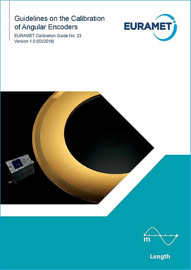
Brand-new guideline from Length area more

Are you keen to broaden your horizons by working abroad – have you considered a Researcher Mobility Grant? more