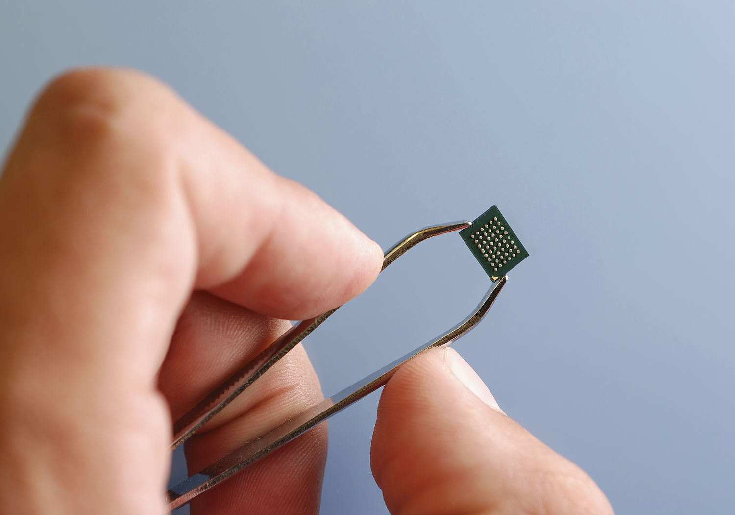
Novel electronic devices based on control of strain at the nanoscale
Short Name: Nanostrain, Project Number: IND54
Characterising new materials for next generation electronics
Europe’s electronics industry, worth hundreds of billions of euros, must innovate to remain competitive as silicon wafers reach their physical limits. Next generation devices will require faster processing speeds, and miniaturised components based on novel materials operating on far smaller scales than current technologies.
Piezoelectric materials have unique properties. When physical forces induce strain, their atomic structure changes – altering their electrical properties. This makes them an ideal candidate for future nanoscale electronic switches. Realising the potential of new materials requires the development of wellcharacterised measurement techniques to accurately determine their properties.
The EMRP project Novel electronic devices based on control of strain at the nanoscale developed advanced analytical techniques for accurately measuring how strain introduces changes in atomic structure. This will support future research into nanoscale piezoelectric materials for next generation electronics. The project:
- Upgraded a facility at the Grenoble XMaS beamline by combining X-rays and lasers for characterising strain at the atomic level. This allows simultaneous measurements of voltage, current, movement, and atomic position changes using X-ray diffraction, making it possible to compare structural changes caused by strain on the nanoscale.
- Demonstrated the measurement of nanoscale stress and strain using infrared optical microscopy and Raman spectroscopy by monitoring interference band changes and relating these to the applied stress.
- Demonstrated and improved Digital Image Correlation (DIC) approaches used to visualise how piezoelectric samples behave under stress, and developed open source software for data analysis.
- Developed theoretical modelling capabilities for predicting how materials change due to strain, based on atomic interactions.
The introduction of next generation microelectronics based on novel materials relies on robust characterisation of their properties on the atomic scale. New measurement techniques must be developed and validated that are suitable for use on a smaller scale than those used today. This project has created world leading European capabilities in characterising materials that are important for next generation electronics, based on improved experimental facilities at the XMaS beamline, operated by the University of Liverpool, and PTB’s synchrotron radiation source. This is evidenced by interest from the US Government in new collaborative research for future radar and quantum communications, as well as IBM’s decision to move a computer research unit to Switzerland.
Research in this area continues in the EMPIR ADVENT project which aims to continue to extend the measurement tools for characterising piezoelectric materials. Longer term, the developments from these new measurement technology projects will stimulate innovation in the electronics industry, ensuring strong European participation in the growth of the nanotechnology market.
Physical Chemistry Chemical Physics
Journal of Applied Physics 121, 055302 (2017); doi: 10.1063/1.4975114
Physical Chemistry Chemical Physics · September 2016
Journal of Physics D: Applied Physics
APL Materials
Review of Scientific Instruments
J. Phys.: Condens. Matter 27 (2015) 475006 (10pp)
The Journal of Physical Chemistry C
Journal Applied Physics
MRS Bulletin
Journal of Materials Chemistry A
Journal of Sol-Gel Science and Technology
